Requirements and considerations for PCB screen printing design
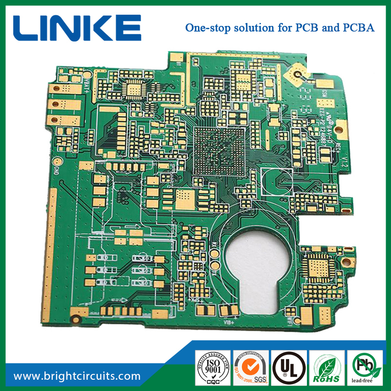
Screen printing design is an essential factor in PCB design. Screen printing on Electronic pcb boards usually includes: component screen printing and tag number, board name, version number, anti-static identification, barcode screen printing, company logo, and other identification. Next, let's take a look at the requirements for screen printing design in PCB design.
Screen printing design requirements:
The ratio of height to width of silk screen characters is generally required to be ≥ 6:1. There are three common font sizes: when the board density is relatively high, 4/25mil characters (size 1) are commonly used; When using regular density, it is recommended to use characters of 5/30mil (number 2); When the board is relatively loose, it is recommended to use 6/45mil characters (number 3); Usually, the thickness of the surface base copper also has corresponding requirements for the screen printing width. The base copper is less than 1OZ, with a limit value of ≥ 4mil and an optimized value of ≥ 6mil; When the thickness of the base copper is 1OZ, priority should be given to using 5/30mil characters; When using base copper 2OZ, prioritize using 6/45mil characters.
Requirements for adding PCB screen printing:
1. Placement: Generally speaking, for the screen printing of devices such as resistors, capacitors, and tubes, do not use four directions when placing them, as this can cause fatigue during debugging, maintenance, and soldering (the board needs to be rotated in several directions).
2. Try not to punch the through-hole on the silk screen.
3. Screen printing should not be pressed on high-speed signal lines (such as clock lines, etc.)
4. The reading direction of silk screen should be consistent with the usage direction, mainly to reduce the probability of reverse soldering during soldering.
5. The pin number should be clearly marked on the silk screen.
6. Screen printing for special packaging: For special packaging such as BGA and QFN, the size of the screen printing should be completely consistent with the size of the chip.
7. Screen printing of installation holes: Screw screen printing has been added near the installation holes, indicating the length and total number of screws for easy installation.
Notes on silk screen design:
1. The screen printing line width on the board should be ≥ 4mil to avoid a screen printing line width of 0 for components.
2. Screen printing and pad spacing: Screen printing should not cover the welding points on the board, such as the through-holes of SMD pads and inserts. Screen printing is made of insulating material, and once the pads are installed, it will lead to poor welding; Also, do not cover the test points, mark points, etc. on the board; Usually, it is required to maintain a spacing of 6mil.
3. Spacing between silk screens: Maintain a distance of 6mil. Overlapping between silk screens is acceptable, but if the overlap results in unrecognizability, it needs to be adjusted.
4. Screen printing direction: The arrangement of screen printing strings should follow the principle of facing the string from left to right or from bottom to top.
5. Device tag placement: The device tag should correspond one-to-one with the device and cannot be reversed or changed in order; When the device density is relatively high, the tag can be placed in other areas on the board with space by using the method of lead out labeling or symbol labeling.
6. The polarity identification of components and the "1" pin identification should be placed correctly and clearly.
7. When introducing annotations or symbol annotations, the added silk screen and characters should be placed on the silk screen layer of Board Geometry.
The added board name, version number, and screen printing are also placed on the screen printing layer of Board Geometry.
8. The device tag number cannot be placed inside the device or outside the board frame.
9. When the board density is relatively high and there is really no space to place the slot number, it can be discussed with the customer not to use the slot number, but assembly drawings need to be provided to facilitate component installation and inspection.
10. When the customer requests to write copper characters on the top and bottom layers, the copper character line width: HOZ base copper - character width above 8mil, height above 45mil; 1OZ base copper - characters with a width of more than 10mil and a height of more than 50mil. At the same time, it is necessary to do a good job of soldermask opening, so that the copper characters on the produced boards are brighter.
Linke Electronics,a professional electronic pcb supplier from China.Welcome to place trial orders from us.
Shijiazhuang Linke Electronics Tech Co.,Ltd
Tel: +86-13603214393
Email: [email protected]
Add: Room 1517,Building A,Lecheng Business Plaza,Huai'an west road,Qiaoxi district, Shijiazhuang City,Hebei Province,China.