PCB board is also called printed circuit board, it can realize the mutual connection between electronic components. PCB board can be used in different industries of electronic products, it plays an important role. So what are the components of the PCB board?
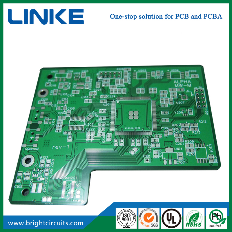
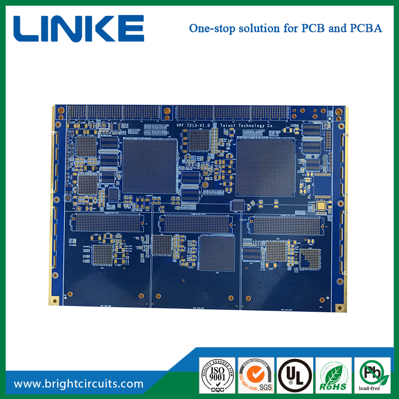
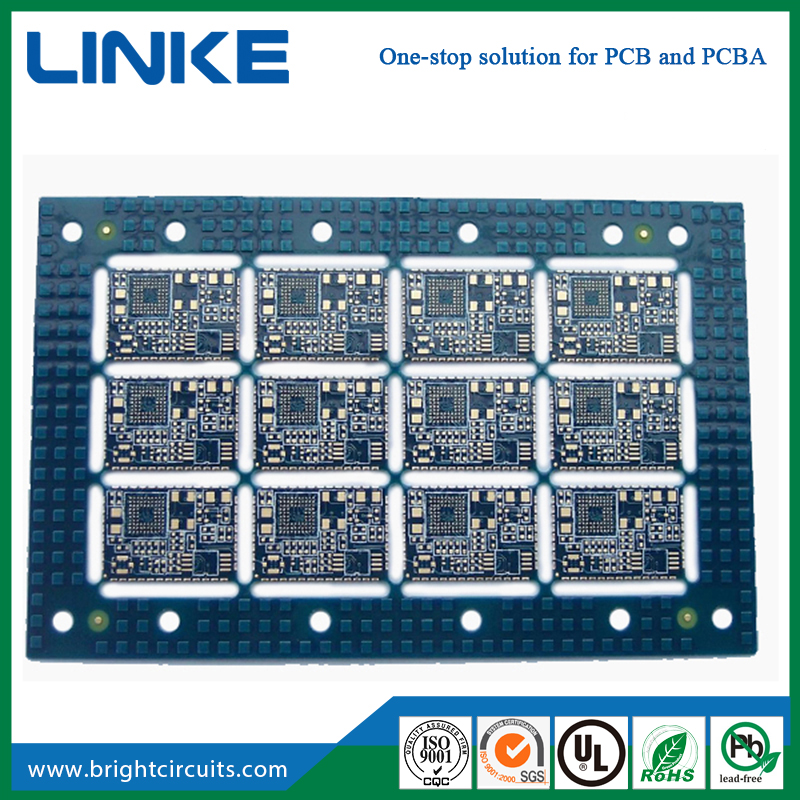
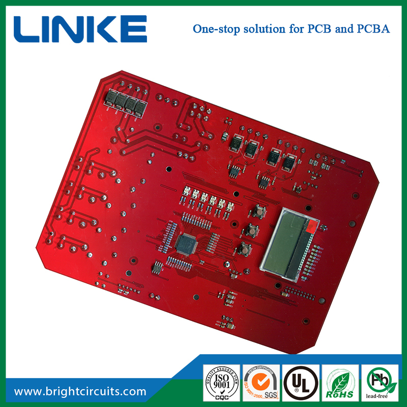
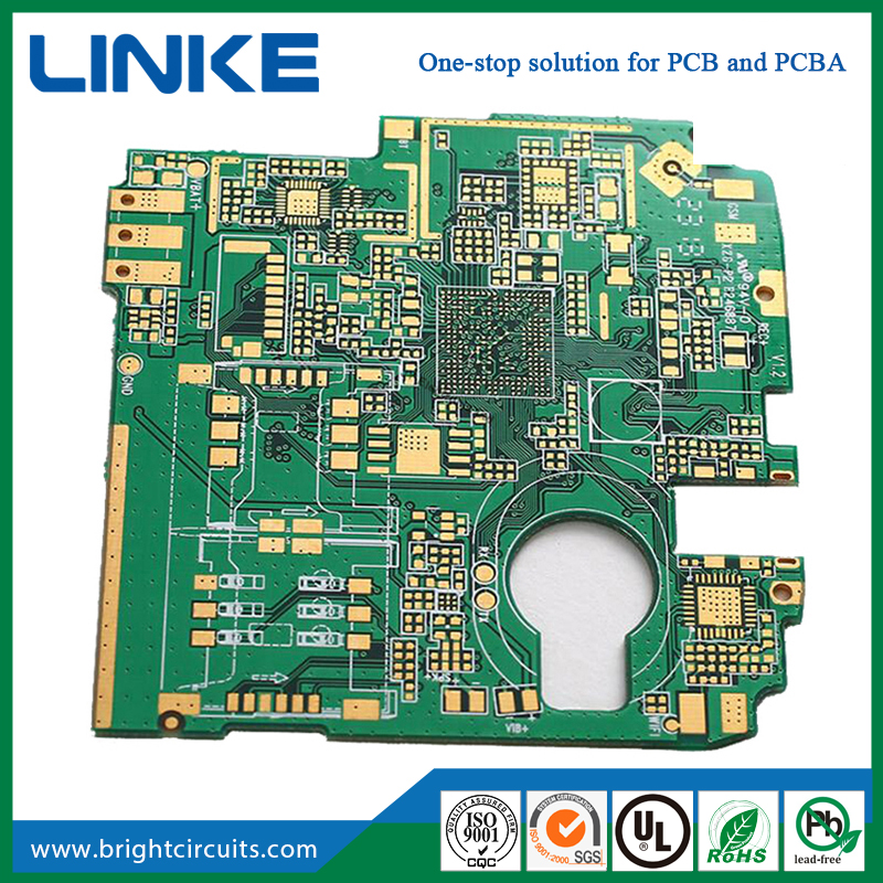
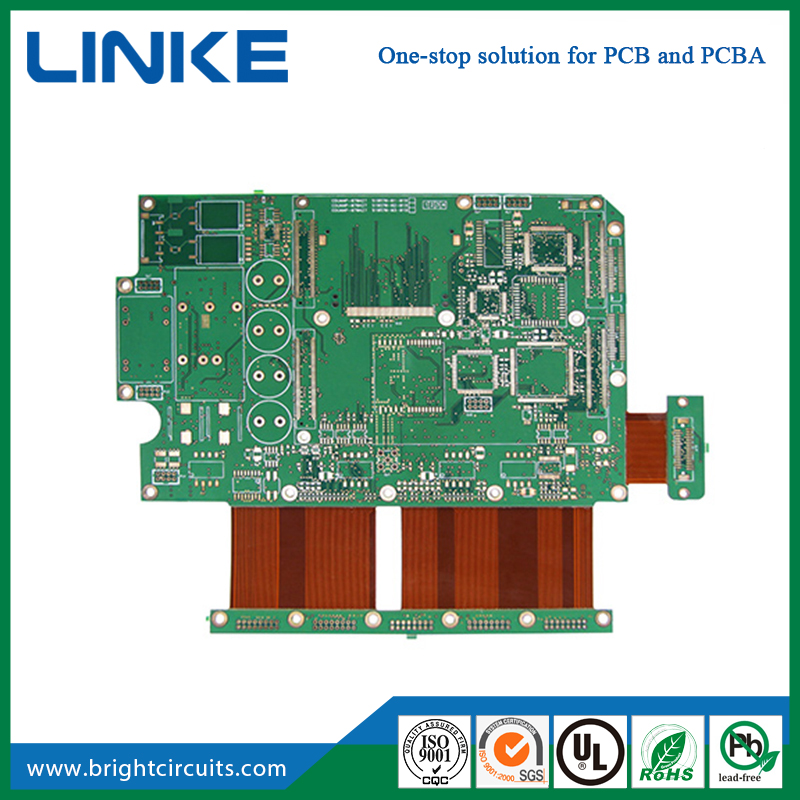
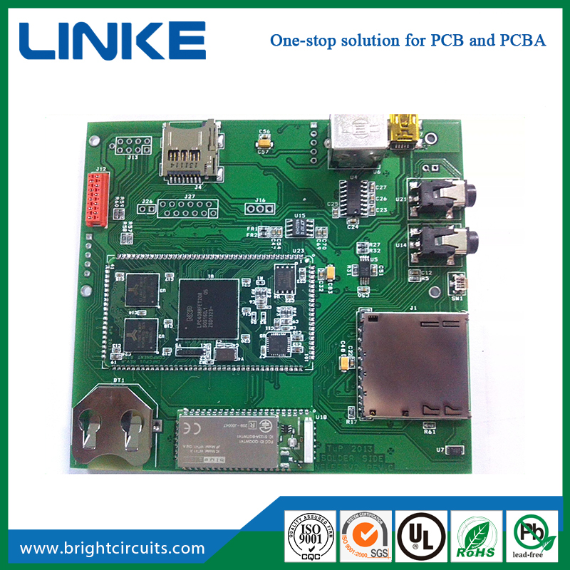
PCB circuit board is composed of: pattern, dielectric, through hole, solder resistant , silk screen and surface Finish.
1. Pattern: Circuit is a tool for conducting between the original parts. In the design, the large copper surface will be designed as the grounding and power supply layer. The circuit is made at the same time as the Pattern.
2. Dielectric layer (Dielectric): it is used to maintain insulation between the circuits and layers, commonly known as substrates.
3. Through hole / via: Through holes can make the circuits more than two layers switch on each other, the larger ones are used as through hole parts soldering, and the non-through holes (nPTH) are usually used as surface mounting positioning and fixing screws for assembly.
4. Solder resistant / Solder Mask: It is not all copper will be soldered by components, so the non-tin area will printed by epoxy resin, it avoids short circuit between non-tin lines. According to different processes, it can be divided into green oil, red oil and blue oil.
5. Legend / Marking/Silk screen: It is not necessary. The main function is to mark the name and position frame of each part on the circuit board. It is easy to maintain and identify after assembly.
6. Surface Finish: Because copper surface in the general environment, it is easy to oxidize, and it leads to no tin (solder poor), so it need protection on these area. The methods of protection include HASL, ENIG, Immersion Silver, tin, Immersion Tin, and OSP, which have their advantages and disadvantages; they are generally called Surface Finish.
FAQ:
1. How to Get a quotation?
For PCBs,pls send us the Gerber File.For PCBA,pls send us the Gerber file and BOM(Bill of Materials)
2. What is the MOQ?
No MOQ.1 pcs is ok.
3.What is the lead time?
For PCB orders,the lead time is 2 to 10 days.For PCBA orders,the lead time will be 15 to 30 days.
4.Will the boards be tested before shippment?
Yes,all PCBs will be tested by Flying Probe or E-test.For PCBA,we will have AOI,X-ray,and functional test