Manufacturing process of Multi-layers PCB
With more and more functions of electronic products, the structure of PCB circuit board is becoming more and more complex. Due to the space limitation of PCB board, PCB is evolving from single layer to double layer and to multilayer. What is the manufacturing process of the multilayer PCB circuit board? Let me introduce.
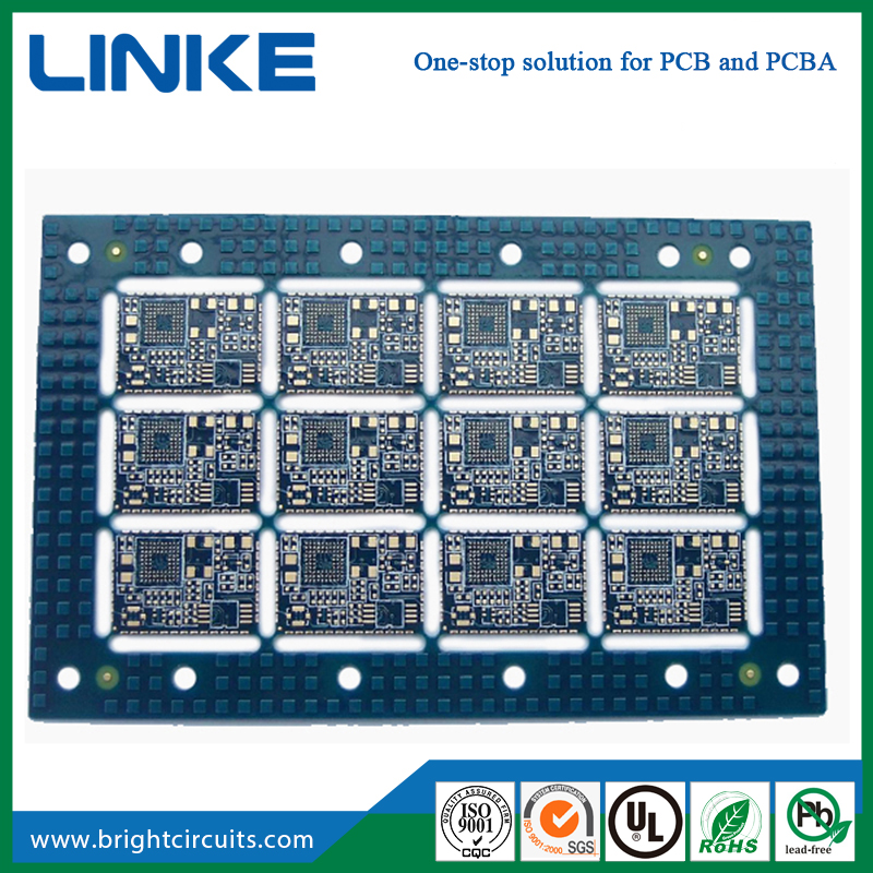
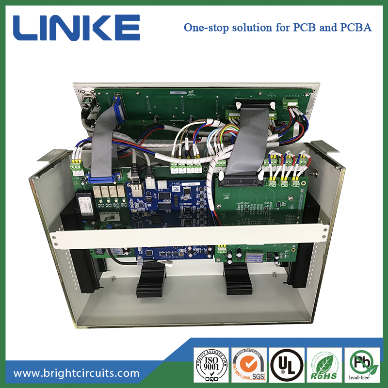
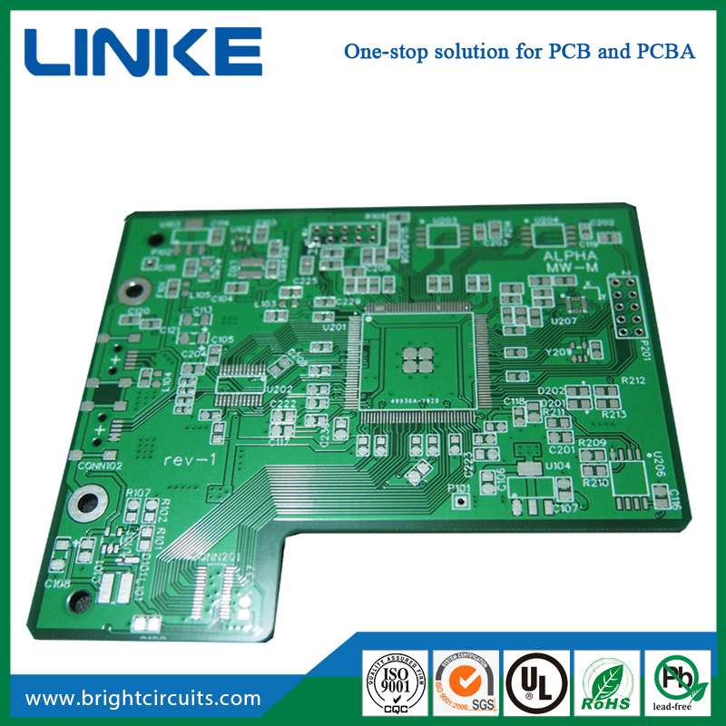
Multilayer PCB circuit board is a kind of printed circuit board composed of alternating conductive pattern layer and insulating material laminated. The electrical interconnect between layers is realized by metallizing holes. If you use a double sided board as the inner layer, two single sided boards as the outer layer or two double sided boards as the inner layer, two single sided boards as the outer layer, and two single sided boards as the outer layer, which are pressed together through the positioning system and the insulating bonding material, and the conductive patterns are interlinked according to the design requirements. It becomes a four-layer, six-layer printed circuit board, also known as a multilayer PCB circuit board.
The multilayer PCB circuit board is usually made of epoxy glass cloth coated copper foil laminates. The manufacturing process is developed on the basis of coated holes on double sided boards. The process is to etch the pattern of the inner laminate. After black oxide, the semi-solidified sheet is added to the predetermined design for lamination. Then it should put a piece of copper foil on the upper and lower surface. The press is heated and pressurized. "Double sided copper clad board" has been prepared, and then the NC drilling is carried out according to the pre-designed positioning system. After drilling, the hole wall should be treated with concave erosion and decontamination, and then it can be carried out according to the technology of double sided coated hole printed circuit board.
Compared with the conventional multilayer and double sided board production process, the multilayer board adds several unique process steps. In most of the processes, some process parameters, equipment accuracy and complexity are different. For example, the metallization connection of the inner layer of the multilayer is the decisive factor. The quality requirement of the hole wall is more strict than that of the double sided board, so the requirement for drilling is even higher.
In addition, the number of stacked boards per drilling, the bit speed and feed rate are different from double sided board. Multilayer and semi-finished products are also more rigorous and complex than double sided boards. Because of the complex structure, the multilayer board should adopt the glycerol hot melt process with uniform temperature. It should not adopt the infrared hot melt technology which may cause the local temperature rise too high.
Multilayer PCB circuit board is the product of high speed, multifunction, large capacity and small volume of electronic technology. As a professional multilayer PCB line manufacturer, we will continue to improve the production process and strive for the rise of the national entity manufacturing industry.