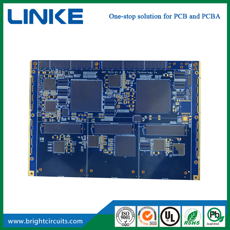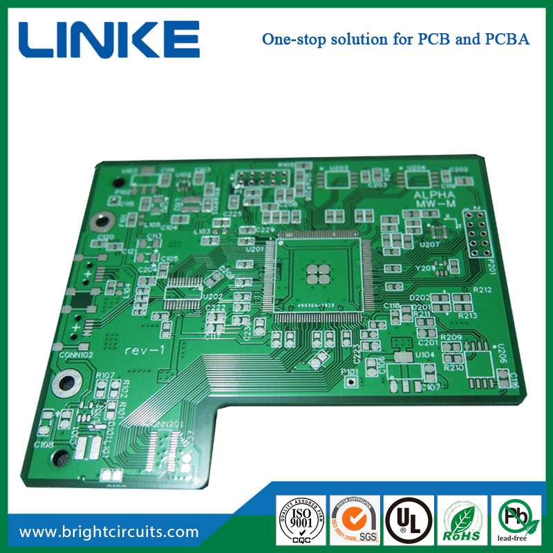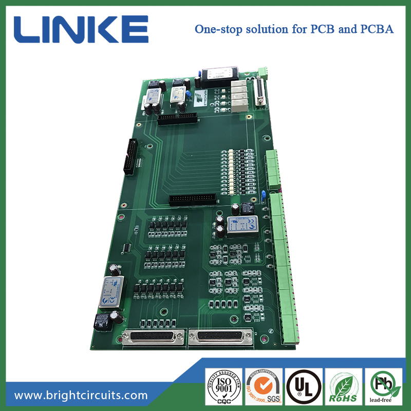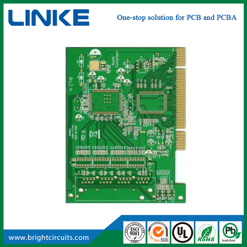
Gold Finger
On computer memory sticks and graphics cards, we can see a row of golden conductive contacts, which are called "golden fingers". The Gold Finger (or Edge Connector) in the PCB design and production industry uses the plug-in of the connector as the outlet for the board to connect to the network. Next, let's understand how to deal with gold fingers in PCB and some details.
The surface treatment method of gold fingers PCB:
1. Electroplating nickel gold: thickness up to 3-50u", due to its superior electrical conductivity, oxidation resistance and wear resistance,it is widely used on gold finger PCBs that require frequent insertion and removal or PCB boards that require frequent mechanical friction.
However, due to the extremely high cost of gold plating, it is only used for partial gold plating such as gold fingers.
2. Immersion gold: The thickness is conventional 1u", up to 3u" because of its superior conductivity, flatness and solderability, it is widely used in high-precision PCB boards with button positions, bonded IC, BGA, etc. Gold finger PCBs with low wear resistance requirements can also choose the entire board immersion gold process, which is much lower than the electro-gold process cost. The color of the Immersion Gold process is golden yellow.
Gold finger detail processing in PCB:
1) In order to increase the wear resistance of the gold finger, the gold finger usually needs to be plated with hard gold.
2) Golden fingers need to be chamfered, usually 45°, other angles such as 20°, 30°, etc. If there is no chamfer in the design, there is a problem.
3) The gold finger needs to be treated as a whole piece of solder mask to open the window, and the PIN does not need to open the steel mesh;
4) Immersion tin and immersion silver pads need to be at a minimum distance of 14mil from the top of the finger; it is recommended that the pad be designed to be at least 1mm away from the finger, including via pads;
5) Do not cover the surface of the gold finger with copper;
6) All layers of the inner layer of the gold finger need to be cut copper, usually the width of the cut copper is 3mm larger; it can be used for half-finger cut copper and whole finger cut copper.
Shijiazhuang Linke Electronics Tech Co.,Ltd
Tel: +86-13603214393
Email: [email protected]
Add: Room 1517,Building A,Lecheng Business Plaza,Huai'an west road,Qiaoxi district, Shijiazhuang City,Hebei Province,China.