Exploring BGA Package Soldering: Common Soldering and Anomaly Analysis
BGA (Ball Grid Array) package is a surface-mounted package that is widely used in the electronics industry for its high density and high performance. However, various defects and abnormalities may occur during the BGA package soldering process. Let's take a look at these common problems and their causes.
Solder ball breakage: Solder ball breakage is a common problem in the BGA soldering process, mainly due to improper control of soldering temperature or equipment vibration. If the soldering temperature is too high, the solder ball may over-expand, leading to ball breakage; if the equipment vibration is too high, it may also lead to increased mechanical stress on the solder ball, which may cause breakage.
Faulty soldering: Faulty soldering is another common problem, mainly manifested as the failure to form a good metal connection at the soldering points. The main reasons for Faulty soldering include poor wetting of the solder, soldering temperatures lower than the melting point of the solder paste, or contamination of the solder during the soldering process.
Solder ball Deflection: During the soldering process, due to thermal expansion and uneven surface tension, the solder ball may deflect, leading to a decrease in connection quality. Especially in high-density BGA packaging, small deviations of solder balls can lead to serious performance issues.
Bridging: If there is too much solder or excessive flow of solder, a bridging connection may form, i.e. an electrical connection between two or more solder joints that should not exist. The presence of a bridge connection not only affects the normal operation of the circuit, but may also cause a short circuit and damage to the equipment.
Post-solder cracking: Post-solder cracking is cracking that occurs during or after soldering, which is caused by soldering stress, thermal cycling stress, or mechanical vibration. Such cracks may cause circuit breakage and affect the reliability of the equipment.
Appearance defects: During the BGA soldering process, appearance defects such as unevenness of the solder surface and darkening of the solder color may occur. These defects are generally caused by improper setting of soldering process parameters, poor control of ambient temperature and humidity, or solder quality problems. Although these defects do not necessarily directly affect the function of the PCB board, but may affect the life and reliability of the PCB board.
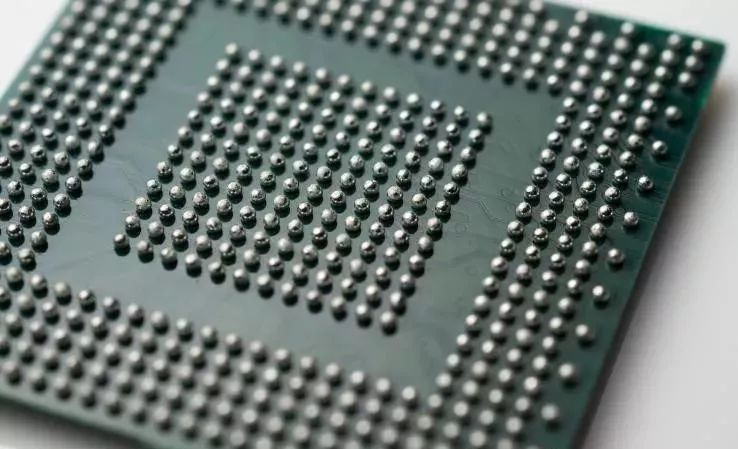
Internal defects: Using X-ray or other non-destructive testing techniques may reveal internal defects in BGA welding, such as holes and cracks inside the solder balls. These internal defects may affect the electrical performance of the circuit and reduce its resistance to fatigue and vibration.
Poor electrical performance after soldering: Some defects may not be directly detected through visual or X-ray inspection, and can only be detected during electrical performance testing. For example, if the soldering quality is poor, it may lead to problems such as increased resistance, current disturbance, signal delay, etc. These issues may seriously affect the performance of the circuit board, and even cause the circuit board to malfunction.
There are many common defects and anomalies in BGA packaging soldering, and each type of defect and anomaly may affect the performance and reliability of the circuit board. Therefore, the control of BGA soldering process is very important, requiring strict process parameter settings, high-quality soldering materials, precise soldering equipment, and strict quality inspection and control. By deeply understanding the common defects and anomalies in BGA packaging soldering, we can better control the soldering process, improve the quality and reliability of circuit boards.
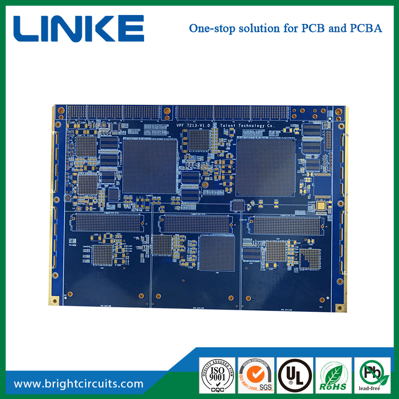
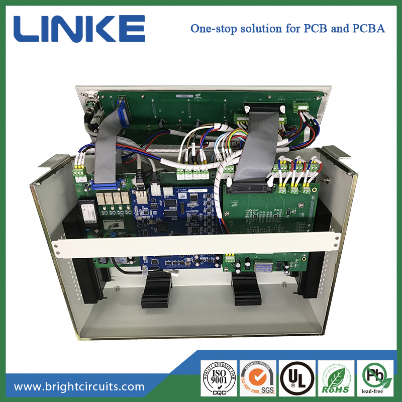
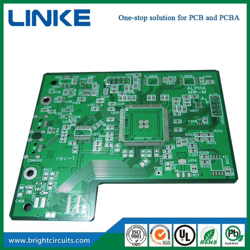
Linke Electronics,a professional PCB assembly BGA assembly supplier from China.Welcome to place trial orders from us.
Shijiazhuang Linke Electronics Tech Co.,Ltd
Tel: +86-13603214393
Email: [email protected]
Add: Room 1517,Building A,Lecheng Business Plaza,Huai'an west road,Qiaoxi district, Shijiazhuang City,Hebei Province,China.